CALL NOW!
What is the Gold Finger?
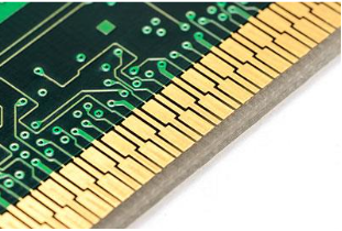
Gold finger is the connector at the edge of boards. It is similar to fingers, so we called gold finger, please see the following pictures. It is used to protect the printed circuit board prototypes from wear and tear.
The surface treatment of the gold finger PCB
Electroplated nickel gold: Thickness up to 3-50u", due to its superior conductivity, oxidation resistance and wear resistance, it is widely used in gold finger PCB that require frequent plugging or PCB board that require frequent mechanical friction.

Immersion Gold: The thickness of conventional is 1u", up to 3u". It is widely used in high-precision PCB board with button position, bonded IC, BGA, etc. due to its superior conductivity, flatness and solderability.
PCB Capabilities
Design Considerations for Gold Finger
The gold finger PCB with low wear resistance requirements can also choose the entire board immersion gold process. The cost of the immersion gold process is much lower than that of the electric gold process. The color of the immersion gold process is golden yellow.
When you see a shape and package similar to the one shown below in the PCB design, the first reaction is that the board has gold finger. A simpler method for judging the golden finger: the TOP and BOTTOM sides of the device both have PIN devices and there will be a u-shape groove as shown below.
When there are gold fingers on the board, it is necessary to handle well the details of the gold finger.
Detail Processing of Gold Finger in PCB:
1) For PCB boards that need to be inserted and removed frequently, gold fingers usually need to be plated with hard gold in order to increase the wear resistance of gold fingers.
2) The gold finger needs to be chamfered, usually 45°, and other angles such as 20°, 30°, etc. If there is no chamfer in the design, there is a problem. As shown below, the arrow shows a 45° chamfer.
3) The gold finger needs to do a whole piece of solder mask window treatment, and the PIN does not need to open the steel mesh;
4) Immersion tin and immersion silver pad need a minimum distance of 14 mil from the tip of the finger. It is recommended that the pad be 1 mm or more away from the finger position, including the via pad;
5) Do not lay copper on the surface of the gold finger.
Have Questions?
If you have any questions or need any further information, please feel free to contact your dedicated customer service.
Provide best in class solutions through engineering excellence and personalized service that exceeds our clients’ expectations.
Services
Get In Touch
Address:
17506 Murphy Parkway
Lathrop, CA 95330
U.S.A
Office: 833-722-3539
Email: Sales@AlteraFlex.com

SGS CN15/30057
SGS CN15/30242
SGS CN15/30241
© 2024 Content, including images, displayed on this website is protected by copyright laws. Downloading, republication, retransmission, or reproduction of the content on this website is strictly prohibited.
TERMS OF USE
|
PRIVACY POLICY
|
ACCESSIBILITY
| Website Built by
BROADPROXIMITY
We use cookies to ensure that we give you the best experience on our website. To learn more, go to the Privacy Page .