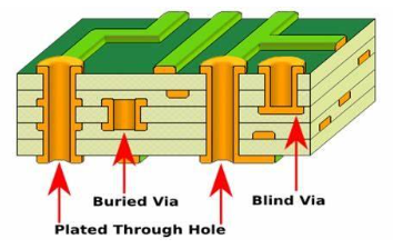
Blind Vias and Buried Vias
Blind and buried vias are only available on boards with at least four layers. Unlike regular vias on a two layer board which connect the two surface layers, buried and blind vias connect the inner layers with either other adjacent inner layers or adjacent surface layers.
Blind Vias:
Connects an inner layer with the adjacent surface layer, they are only visible on one side of the boards and so are called 'blind' vias.
Buried Vias:
Connects two adjacent inner copper layers. They are not visible from the surface and so are 'buried'.
Advantages and disadvantages
Using blind and buried vias in a PCB design has its advantages and disadvantages. The advantage, of course is that this technology offers a viable design technique to help meet the density constraints of lines and pads on a typical design without increasing the layer count or board size. The disadvantage of the technology is that due to the additional operations in manufacturing the board, the cost of a board using blind and/or buried vias is significantly higher than a typical multilayer_ board with the same number of layers.
Have Questions?
If you have any questions or need any further information, please feel free to contact your dedicated customer service.
