Surface Finish
At present, the environmental problems involved in PCB production are particularly prominent. Lead and bromine are the hottest topics at the moment.
Surface Finish Technology
Lead-free and halogen-free will affect the development of PCB in many ways. Although changes in the surface treatment process of PCB are not significant at present and seem to be relatively distant, it should be noted that the slow change in the long term will lead to great changes.
PCB surface treatment technology is bound to change dramatically in the future as environmental concerns grow.
PCB surface finish is a coating between a component and a bare board PCB. It is applied for two basic reasons: to ensure solderability, and to protect exposed copper circuitry. As there are many types of surface finishes, selecting the right one is no easy task, especially as surface mounts have become more complex and regulations such as RoHS and WEEE have changed industry standards. Recently, the common PCB surface treatment technologies which we PCBWay may use when manufacturing PCBs are HASL(hot air solder leveling), organic coating (OSP), electroless nickel/gold, electroless silver, electroless tin, etc.
HASL (hot air solder leveling)/HASL lead Free:
Hot air solder leveling is the process of coating molten tin-lead solder on the surface of PCB and heating compressed air leveling (blowing), so that it forms a layer of both anti-copper oxidation and good weldability of the coating. PCB shall be immersed in the molten solder during hot air solder leveling.
The air knife shall flush the liquid solder before the solder solidifies, and it can minimize the crescent shape of the solder on the copper surface and prevent the solder bridge.
Hot air rectification is divided into two types
vertical type and horizontal type. Generally speaking, the horizontal type is better, and horizontal type hot air leveling coating is mainly uniform.
The general process of automatic production is as follows:
01>
Micro-Corrosion
02>
Preheating
03>
Coating Flux
04>
Spraying Tin
05
Cleaning
Pros
- Low-cost
- Available
- Repairable
Cons
- Uneven Surfaces
- Not good for fine pitch components
- Thermal Shock
- Not good for plated through-hole (PTH)
- Poor wetting
Organic Coating (OSP):
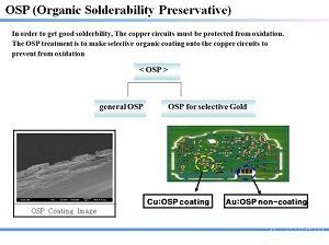
Unlike other surface treatment processes, OSP acts as a barrier between copper and air. In simple terms, OSP is a chemical process to grow a layer of organic skin film on the clean bare copper surface, which has anti-oxidation, heat shock and moisture resistance, to protect the copper surface from rust (oxidation or vulcanization, etc.) in the normal environment. At the same time, it must be easily removed by the flux in subsequent welding temperatures for welding. The organic coating process is simple, low cost, make it widely used in the industry. The early organic coating molecules are the anti-rust imidazole and benzotriazole, and the most recent molecules are mainly benzimidazole.
To ensure that multiple reflows can be performed
it might not work if there was only a single layer of organic coating on the copper surface, that’s to say, there must be many organic layers, which is why the copper solution is usually added to the chemical bath.
After coating the first layer, the coating layer adsorbs copper, and then, the second layer of organic coating molecules bind to copper until twenty or even hundreds of organic coating molecules concentrate on the copper surface.
The Organic Coating Process:
01>
Degrease
02>
Micro-Etching
03>
Pickling
04>
Pure Water Cleaning
05>
Organic Coating
06
Cleaning
Pros
- Lead-free
- Flat surface
- Simple process
- Repairable
Cons
- Not good for PTH
- Sensitive
- Short Shelf life
ENIG (Electroless Nickel/Immersion Gold):
Unlike OSP, ENIG only is a thick nickel gold alloy with excellent electrical properties on the copper surface and can protect PCB for a long time and acts as a rust barrier, which can be useful and achieve good electrical performance in the long term use of PCB. What’s more, it also has environmental tolerance than other surface treatment processes do not. Nickel plating is because gold and copper diffuse to each other, and the nickel layer can prevent the diffusion between them.
Without the nickel layer, gold will spread to the copper within hours. Another benefit of electroless nickel/impregnation is the strength of nickel, which is only 5um thick to control Z expansion at high temperatures. Besides, electroless nickel/gold plating can also prevent copper from dissolving, which will be beneficial for lead-free welding.
ENIG (Electroless Nickel/Immersion Gold):
01>
Pickling Cleaning
02>
Micro-Etching
03>
Pre Leaching
04>
Activation
05>
Electroless Nickel Plating
06
Chemical Leaching
Pros
- Flat surfaces
- Strong
- Lead-free
- Good for PTH
Cons
- Black pad syndrome
- Expensive
- Not good for rew
Characteristics of common surface treatment methods
| physical property | Sn-Pb HASL | Immersion silver | Immersion Tin | OSP | Immersion gold (ENIG) |
|---|---|---|---|---|---|
| Shelf life (month) | 18 | 12 | 6 | 6 | 24 |
| Reflow times | 4 | 5 | 5 | 4 | 4 |
| Cost | medium | medium | medium | low | high |
| Process Complexity | high | medium | medium | low | high |
| Process temperature | 240°C | 50°C | 70°C | 40°C | 80°C |
| Thickness range (um) | 1-25 | 0.05-0.20 | 0.8-1.2 | 0.2-0.5 | 0.05-0.2 Au 3-5 Ni |
| Flux compatibility | Good | Good | Good | general | Good |
| Environmental protection | No | Yes | Yes | Yes | Yes |
| Others | Thickness Nonuniformity | Easily scratched | Short storage | Sensitive to environment | Easily-broken interface |
Have Questions?
If you have any questions or need any further information, please feel free to contact your dedicated customer service.


