Silkscreen
The silkscreen layer is the top layer of the PCB and serves as a reference indicator for placing components on the PCB. The graphics and text on PCB a circuit board is usually printed with a permanent non-conductive epoxy ink. The color is typically white, although other colors are also available.
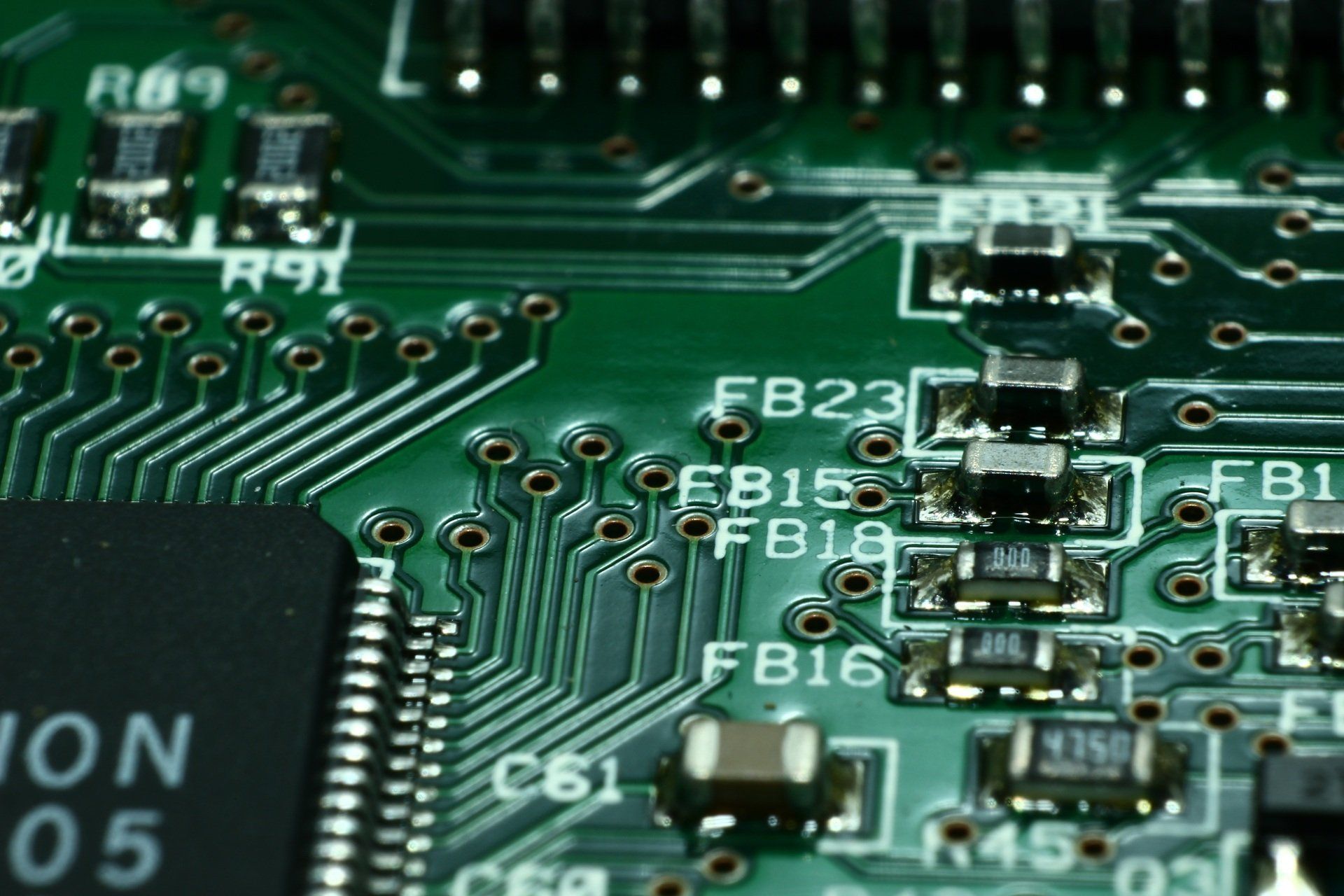
PCB Silkscreen
Screen printing is used to specify useful information on the PCB board, which can help users during the assembly. It is used to mark component values, part numbers, test points, polarity, etc. The problems related to the material of silkscreen are rarely occurred, except maybe some discoloration after high PCB reflow temperatures for RoHS compliant soldering.

Silkscreen problems are always caused by the design of the PCB. So the following part will take some time to mention a few guidelines of the silkscreen design. If silkscreen epoxy is printed over lands PCB or pads that will be soldered, it will melt into the solder joint during reflow and weaken the attachment.
Many CAD systems can clip the silkscreen away from exposed metal
But when creating library components be sure to keep the component outlines and polarity marks away from the pins (0.25mm) by default, and pay attention when moving or rotating reference designators or when adding text to PCB the final board design.
The width of silkscreen graphics can also be a problem. If too thin, we will have problems in the screening or printing process and skips can occur. If too thick, the text may be too blurry to read. As components get smaller in size and circuit density continues to increase, it is sometimes very difficult to print silkscreen at all, but try to use line widths not less than 0.15 mm (6 mils), 0.18 mm to 0.20 mm is preferred PCB.
Solder pads should never be overprinted
because this may lead to problems during soldering, assembly, and with the E-Test. If we should detect an overprinted solder pad (spacing < 150μm), then Multi-CB reserves the right to remove the marking print at this location. Relevant for the definition of the solder pads is the solder pad exemption. The marking print is usually automatically clipped with a spacing of 100μm to the solder-stop edge.
The spacing between solder pad and marking print should be at least 150μm. Always avoid overprinting solder pads!
Silkscreen printing method
| Productivity | For high / mass production |
| Material cost | Cheap |
| Coating thickness | It is relatively thick, but it gets scattered |
| Resolution | Bleeding occurred |
| Silk color | White, black, yellow |
It is a printing method using a plate material with chemical fibers in a mesh form. By rubbing ink with a squeegee, ink is pushed out between the meshes and printed on the board. For silk printing of printed circuit boards, it is a general construction method.
Inkjet method
| Productivity | Low |
| Material cost | Expensive |
| Coating thickness | It is thicker but different |
| Resolution | good |
| Silk color | White / Black |
This is a printing method that absorbs ink by directly spraying onto a substrate. This is an environmentally friendly method because no sheets or films are used. The print resolution is higher than "screen printing". Inkjet white inks may have a slightly milky "milky" appearance.
There are three main ways to add silkscreen coating on a PCB:
Manual screen-printing
Professional R&D on high density HDI, multi-layer PCB, rigid-flex PCB. Embedding technology of small size core, thick GEM, PCB with special requirements from industries like Telecom / medical / automotive, and etc.
Liquid Photo Imaging (LPI)
This process provides more accuracy and legibility over manual screening and is used when line widths are greater than 4 mm
Direct Legend Printing (DLP)
This is the most accurate way of adding a silkscreen, however, it is very expensive.
