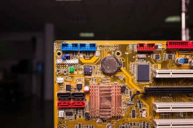
Thick-Copper PCBs
Heavy Copper also known as thick copper PCBs is characterized by structures with copper thicknesses from 105 to 400 µm. These PCBs are used for large (high) current outputs and optimization of thermal management.
Thick-Copper PCBs
The thick copper allows large PCB-cross-sections for high current loads and encourages heat dissipation. The most common designs are multilayer or double-sided.
With this PCB technology it is also possible to combine fine layout structures on the outer layers and thick copper layers in the inner layers.

Performance of Thick Copper PCB:
Thick copper PCB has the best elongation performance and is not limited by the processing temperature. It can be used in hot melt welding methods such as oxygen blowing at a high melting point and not brittle at low temperatures. Even in extremely corrosive atmospheric environments, copper PCB forms a strong, non-toxic passivation protective layer.
Advantages of Thick Copper PCB:
Thick copper PCB is widely used in various household appliances, high-tech products, military, medical and other electronic equipment. The application of thick copper PCB makes the core component of electronic equipment products-circuit boards have a longer service life, and at the same time it is very helpful to the size reduction of electronic equipment
In PCB prototype, thick copper PCB belongs to a special technology, has certain technical thresholds and operating difficulties, and is relatively expensive. At present, in the process of PCB prototype, AlteraFlex can achieve 1-30 layers, the maximum copper thickness is 13oz, the minimum hole size is 0.15 ~ 0.3mm.
Check AlteraFlex Thick PCB Manufacturing Capabilities in The Following Table:
| Feature | Capability |
|---|---|
| Material | FR-4 Standard Tg 140°C, FR4-High Tg 170°C |
| Min. Track/Spacing | For External layers: 4oz Cu 10mil/13mil,5oz Cu 12mil/15mil 6oz Cu 15mil/15mil, For Internal layers: 4oz Cu 8mil/8mil,5oz Cu 10mil/10mil 6oz Cu 12mil/12mil |
| Min. Hole Size | 0.15 ~ 0.3mm |
| Max Outer Layer Copper Weight (Finished) | 13oz |
| Max Inner Layer Copper Weight | 12oz |
| Board Thickness | 0.6-6mm |
| Surface Finishing | HASL lead free,Immersion gold, OSP, Hard Gold,Immersion Silver,Enepig |
| Solder Mask | Green, Red, Yellow, Blue, White, Black, Purple, Matte Black, Matte green |
| Silkscreen | White, Black |
| Via Process | Tenting Vias,Plugged Vias,Vias not covered |
| Testing | Fly Probe Testing (Free) and A.O.I. testing |
| Build time | 5-15 days |
Have Questions?
If you have any questions or need any further information, please feel free to contact your dedicated customer service.
