Printed Circuit Board (PCB) Assembly Services Process
PCB assembly is a highly professional and complex process. Not only involves advanced production equipment, and advanced production process but also needs professional engineering and technical personnel and an excellent production management system. AlteraFlex has the production equipment and has assembled a production team to develop products that exceed expectations.
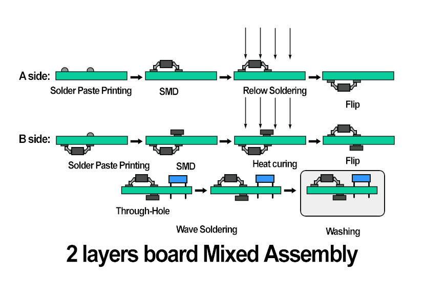
Surface Mount Assembly Process
Required Elements
The following are the required elements for auto assembly:
Quantity Per Part Number
Gerbers in 274-X (embedded apertures) including fabrication drawing.
Part centroid text file with Reference Designators, external placement layer, and X & Y location and rotation in ASCII format.
Numerical control (NC) drill files
Solder paste file (one of the Gerber files) for all sides mounted
Glue dot file
If possible, the design database, specifying the database format (program name)
Parts list or BOM (bill of material)
1. Ordering a Board
AlteraFlex One-Stop Solution for PCB & Prototype Assembly,
2. DFM Check
The DFM check looks at all the design specifications of a PCB. Specifically, this check looks for any missing, redundant or potentially problematic features. Any of these issues may severely and negatively influence the functionality of the final project. For example, one common PCB design flaw is leaving too little spacing between PCB components. This can result in shorts and other malfunctions.
3. IQC of Purchased Components
AlteraFlex Verifying all incoming materials and handling quality problems before subsequent SMT assembly begins. Our IQC position will check following issues of incoming materials if they comply with our strict requirements.
- Model number and quantities according to BOM list
- Shape (deformation, broken pin, oxidation etc), particularly for IC or other complex components
- Sample test of incoming materials by tools such as test frame, multimeter etc.
- If above defect or discrepancy occurs, we will return full incoming materials to supplier or customer.
4. Machine programming - Gerber / CAD to Centroid / Placement / XY file
Having received the PCB panels and components the next step is to setup the various machines used with the manufacturing process. Machines such as the placement machine and AOI (Automated Optical Inspection) will require a program to be created which is best generated from CAD data but quite often this isn't available.
Gerber data is almost always available as this is the data required for the bare PCB to be manufactured.
5. Solder Paste Printing
The first machine to setup in the manufacturing process is the solder paste printer which is designed to apply solder paste using a stencil and squeegees to the appropriate pads on the PCB.
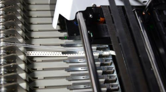
6. Component Placement
Once the printed PCB has been confirmed to have the correct amount of solder paste applied it moves into the next part of the manufacturing process which is component placement. Each component is picked from its packaging using either a vacuum or gripper nozzle, checked by the vision system and placed in the programed location at high speed.

7. Pre-Reflow Automated Optical Inspection (AOI)
Following the component placement process it is important to verify that no mistakes have been made and that all parts have been correctly placed before reflow soldering. The best way of doing this is by using an AOI machine to make checks such as component presence, type/value and polarity.
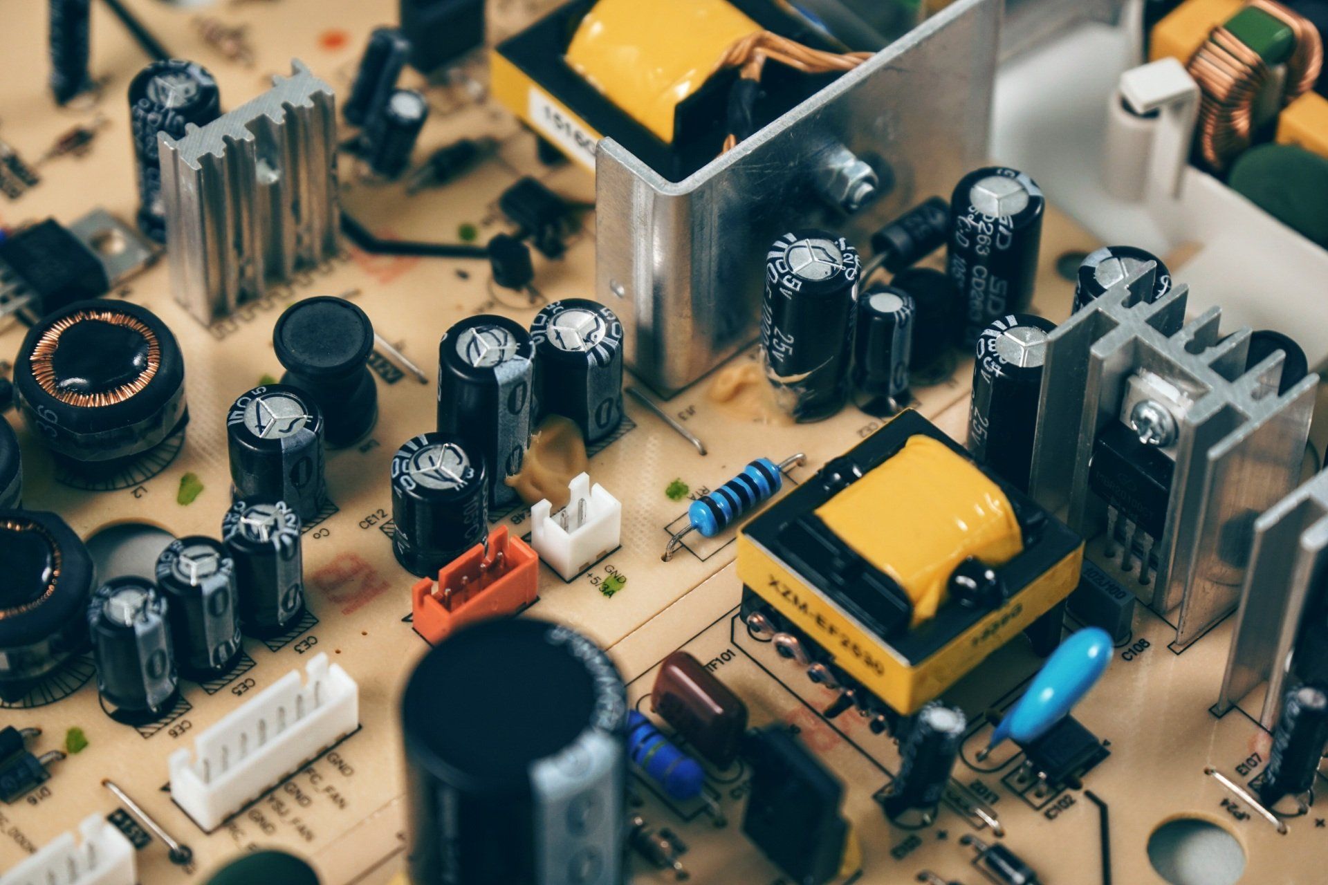
8. Reflow Soldering
Once the components are placed on the boards, each piece is sent through our reflow machines. This means the solder paste needs to solidify, adhering components to the board. PCB assembly accomplishes this through a process called "reflow".
This would appear to be one of the less complicated parts of the assembly processes but the correct reflow profile is key to ensure acceptable solder joints without damaging the parts or assembly due to excessive heat. When using lead-free solder a carefully profiled assembly is even more important as the required reflow temperature can often be very close to many components maximum rated temperature.
9. Post-Reflow Automated Optical Inspection (AOI)
The last part of the surface mount assembly process is to again check that no mistakes have been made by using an AOI machine to check solder joint quality.
Often, movement during the reflow process will result in poor connection quality or a complete lack of a connection. Shorts are also a common side effect of this movement, as misplaced components can sometimes connect portions of the circuit that should not connect. Checking for these errors and misalignments can involve one of several different inspection methods.
The most common of these inspection methods include the following:
- Manual Checks
- Automatic Optical Inspection(AOI)
- Automated X-ray inspection(AXI)
10. Conformal Coating
Some completed Printed Circuit Board Assemblies have a conformal coating. Material -UV40 Coating Thickness -0.003 +/-0.002 Coating Standard -IPC J-STD-001
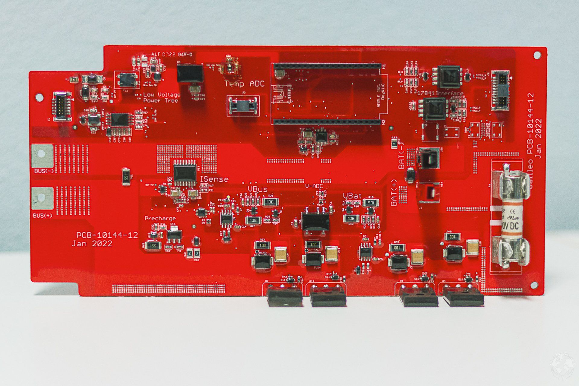
11. Final Inspection and Functional Test
After the soldering and conformal coating step of the PCB assembly process is finished, a final inspection will test the PCB for its functionality by our Quality Assurance team. This inspection is known as a "functional test". The test software and tools are usually provided by the customer, AlteraFlex can also make fixtures according to customer requirements. The test puts the PCB through its paces, simulating the normal circumstances in which the PCB will operate. Power and simulated signals run through the PCB in this test while testers monitor the PCB's electrical characteristics.
12. Washing and Drying
Suffice it to say, the manufacturing process can be a filthy one. Soldering paste leaves behind some amount of flux, while human handling can transfer oils and dirt from fingers and clothing to the surface of the board. Once all is said and done, the results can look a little dingy, which is both an aesthetic and a practical issue.
13. Packing and Shipping
All assembled boards are packaged (can request in anti-static packaging) and shipped DHL,FedEx,UPS,EMS,and so on. Any unused components are returned in accordance with customer instructions. Additionally, customers are notified via email when their packages ships.
Have Questions?
If you have any questions or need any further information, please feel free to contact your dedicated customer service.
